PCB marking machine versus silk-screen printing: what are the advantages and disadvantages? PCBs are used for short circuit boards. PCB as a modern electronic component is one of the most active in the industry, used in almost all electronic products, such as mobile phones, computers, multimeters, and others. With PCB product varieties and batches becoming increasingly complex, product management becomes more challenging for merchants. The marking of characters on the PCB board, barcode and QR code information for traceability has become the industry’s trend to achieve quality control in the manufacturing process.
There are two ways to compare the advantages and disadvantages of PCB laser marking machine and screen printing on the traceability label on the PCB processing. Which has the biggest disadvantage?
Printing way tags for screen printing
Under pressure, make a good graphics screen, allowing character ink to flow through on part of the mesh, and bearing on the circuit board surface. There will be no ink blocking the rest of the screen mesh, only a blank on the circuit board surface, forming a text, logo, design, etc.
A big advantage is the relatively low price and the fast shipping
Negative aspects:
Because ink on the surface of the PCB is easily rubbed off by friction, the image is distorted and easy to fall off.
Removable: by hydrochloric acid and cyclohexanone solution, the PCB can be removed directly from the characters, allowing information to be altered.
There are some rough spots in the silk screen printing on the large PCB board, and the bold font is hard to read.
The organic solvent used in the printing process as well as the heavy metals and other chemicals in the raw materials can cause air pollution, injury to personnel, and health problems.
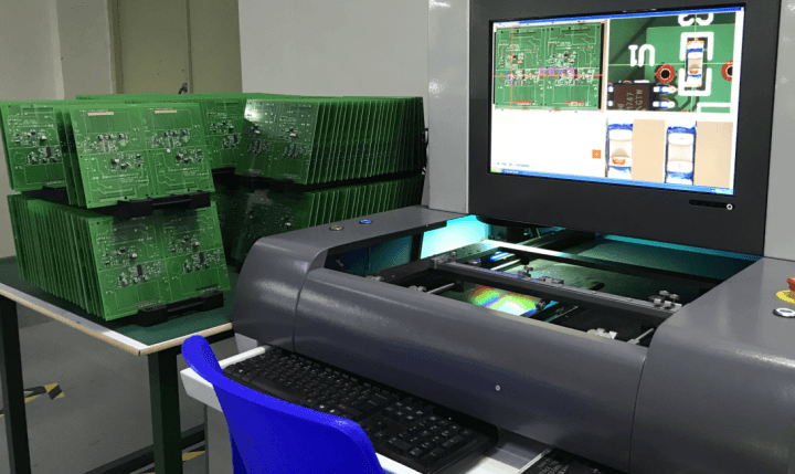
Way tags marked with lasers
The PCB laser marking machine is the use of lasers to irradiate local areas of a PCB, vaporise material on the surface, or change the colour of a chemical reaction, in order to leave a permanent mark of a marking method on the PCB. The laser marking technology can create all kinds of characters, symbols, and motifs, the characters can be as small as a few micrometres, ensuring product security. Benefits:
By laser-direct etching characters, symbols, and permanent characters on the material surface, damage can be resisted.
When the computer graphics are designed correctly, the graphics can be displayed in an instant, no matter what the operation is.
The benefits of laser machining are clear: high accuracy, light weight, can achieve precise marking, clear and beautiful patterns.
Material savings: No contact & throughout; Processing without damaging the workpiece, without damaging the material, reducing material costs.
Environment protection: laser marking does not emit harmful gases, protecting the operator’s safety and working environment.
One weakness is the high upfront costs,
Since the rapid development of electronics manufacturing technology, portable electronic products have become increasingly miniaturised, highly integrated, and light directed. As packaging technology develops, welding plates and spacing shrink, making counterpoint printing more difficult. With its precision and flexibility, PCB laser marking machines can compensate for silk screen printing that is easily damaged, and machining accuracy that isn’t too high, will play an important role in the PCB industry.


More Stories
Choosing the Right Business Loan For Your Company
How Twitter Can Help Your Business
Facebook Small Business Marketing – How To Get More Traction